- 您现在的位置:买卖IC网 > Sheet目录1062 > 101-0506 (Rabbit Semiconductor)CARD CPU SR9160 128K SRAM SMRTST
�� �
�
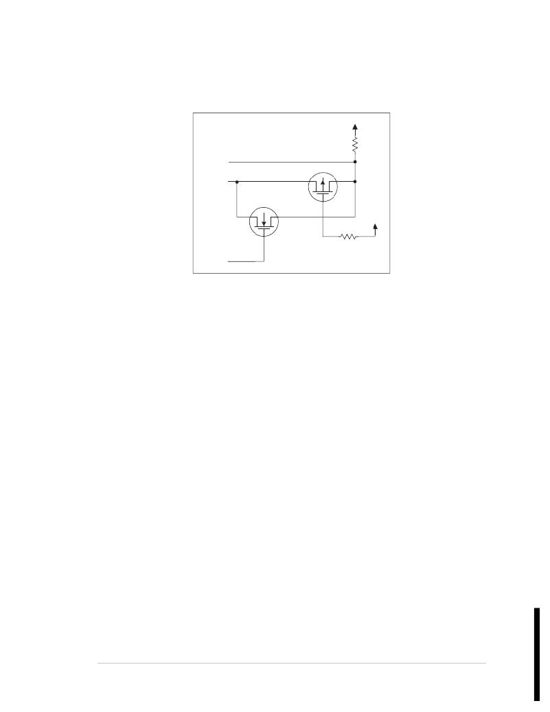
�C.3� Chip� Select� Circuit�
��VRAM�
�R31�
�/CSRAM�
�Q4�
�/CS1�
�Q5�
�VRAM�
�R37�
�10� k� W�
�/RES�
�Figure� C-5.� Chip� Select� Circuit�
�The� current� drain� on� the� battery� in� a� battery-backed� circuit� must� be� kept� to� a� minimum.�
�When� the� CPU� Card� is� not� powered,� the� battery� keeps� the� SRAM� memory� contents� and�
�the� real-time� clock� (RTC)� going.� The� SRAM� has� a� powerdown� mode� that� greatly� reduces�
�power� consumption.� This� powerdown� mode� is� activated� by� raising� the� chip� select� (CS)�
�signal� line.� Normally� the� SRAM� requires� +5� V� to� operate.� However,� only� 2� V� is� required�
�for� data� retention� in� powerdown� mode.� Thus,� when� power� is� removed� from� the� circuit,� the�
�battery� voltage� needs� to� be� provided� to� both� the� SRAM� power� pin� and� to� the� CS� signal�
�line.� The� CS� control� circuit� accomplishes� this� task� for� the� CS� signal� line.�
�In� a� powered-up� condition,� the� CS� control� circuit� must� allow� the� processor� ’s� chip� select�
�signal� /CS1� to� control� the� SRAM’s� CS� signal� /CSRAM.� So,� with� power� applied,� /CSRAM�
�must� be� the� same� signal� as� /CS1,� and� with� power� removed,� /CSRAM� must� be� held� high�
�(but� only� needs� to� be� battery� voltage� high).� Q4� and� Q5� are� MOSFET� transistors� with�
�opposing� polarity.� They� are� both� turned� on� when� power� is� applied� to� the� circuit.� They�
�allow� the� CS� signal� to� pass� from� the� processor� to� the� SRAM� so� that� the� processor� can� peri-�
�odically� access� the� SRAM.� When� power� is� removed� from� the� circuit,� the� transistors� will�
�turn� off� and� isolate� /CSRAM� from� the� processor.� The� isolated� /CSRAM� line� has� a� 100� k� ?�
�pullup� resistor� to� VRAM� (R31).� This� pullup� resistor� keeps� /CSRAM� at� the� VRAM� voltage�
�level� (which� under� no� power� condition� is� the� backup� battery’s� regulated� voltage� at� a� little�
�more� than� 2� V).�
�Transistors� Q4� and� Q5� are� of� opposite� polarity� so� that� a� rail-to-rail� voltage� can� be� passed.�
�When� the� /CS1� voltage� is� low,� Q5� will� conduct.� When� the� /CS1� voltage� is� high,� Q4� will�
�conduct.� It� takes� time� for� the� transistors� to� turn� on,� creating� a� propagation� delay.� This�
�delay� is� typically� very� small,� about� 10� ns� to� 15� ns.�
�The� signal� that� turns� the� transistors� on� is� a� high� on� the� processor� ’s� reset� line,� /RES.� When�
�the� CPU� Card� is� not� in� reset,� the� reset� line� will� be� high,� turning� on� n-channel� Q5.� When� a�
�reset� occurs,� the� /RES� line� will� go� low.�
�User� ’s� Manual�
�171�
�发布紧急采购,3分钟左右您将得到回复。
相关PDF资料
101-0545
PROTOTYPING BOARD FOR LP3500
101-0563
RCM3400 PROTO BOARD
101-0589
CLONING BOARD RABBIT
101-0688
CARD D/A EXPANSION RN1300
101-0954
KIT DEV RABBIT RCM3360/3370 INTL
101-1050-BE-00025
ADPT USB 2 A FEMALE-2 5PIN .25M
10112627-101LF
MINI-SAS HD 1X2 EXT PCB
10112628-101LF
MINI-SAS HD 1X4 EXT PCB
相关代理商/技术参数
101-0507
功能描述:模块化系统 - SOM RCM3000 RABBITCORE
RoHS:否 制造商:Digi International 外观尺寸:ConnectCore 9P 处理器类型:ARM926EJ-S 频率:150 MHz 存储容量:8 MB, 16 MB 存储类型:NOR Flash, SDRAM 接口类型:I2C, SPI, UART 工作电源电压:3.3 V 最大工作温度:+ 85 C 尺寸:1.97 in x 1.97 in x 6.1 in
101-0508
功能描述:模块化系统 - SOM RCM3010 RABBITCORE
RoHS:否 制造商:Digi International 外观尺寸:ConnectCore 9P 处理器类型:ARM926EJ-S 频率:150 MHz 存储容量:8 MB, 16 MB 存储类型:NOR Flash, SDRAM 接口类型:I2C, SPI, UART 工作电源电压:3.3 V 最大工作温度:+ 85 C 尺寸:1.97 in x 1.97 in x 6.1 in
101050-9
制造商:RUKO 功能描述:Bulk 制造商:RUKO 功能描述:STEP DRILL 4-12MMX1MM 制造商:RUKO 功能描述:STEP DRILL, 4-12MMX1MM 制造商:RUKO 功能描述:STEP DRILL, 4-12MMX1MM; Drill Bit Size Metric:4mm; Overall Length:65mm; SVHC:No SVHC (19-Dec-2012); Drill Bit Type:Step; Drill Point Diameter:4mm; Material:HSS; Range:4mm - 12mm; Shank Dia:6mm; Step:1mm ;RoHS Compliant: NA
101050BO
制造商:TE Connectivity 功能描述:
101051
制造商:RUKO 功能描述:STEP DRILL 4-20MMX2MM 制造商:RUKO 功能描述:STEP DRILL, 4-20MMX2MM 制造商:RUKO 功能描述:STEP DRILL, 4-20MMX2MM; Drill Bit Size Metric:4mm; Overall Length:75mm; SVHC:No SVHC (19-Dec-2012); Drill Bit Type:Step; Drill Point Diameter:4mm; Material:HSS; Range:4mm - 20mm; Shank Dia:8mm; Step:2mm ;RoHS Compliant: NA
10-105108-03G
制造商:Amphenol Aerospace 功能描述:10-105108-03G
10-105108-03P
制造商:Amphenol Aerospace 功能描述:10-105108-03P
10-105108-04P
制造商:Amphenol Aerospace 功能描述:10-105108-04P